26/01/2026
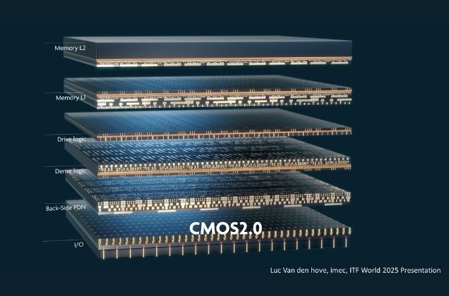
CMOS technology has revolutionized the electronics industry by balancing performance, energy efficiency, and affordability for semiconductor chip fabrication. However, many agree that CMOS technology is now approaching its physical limits. At this point, CMOS 2.0 aims to design functions in multiple 3D stacked layers using specialized chips, representing a new paradigm. Utilizing 3D integration technologies, the CMOS 2.0 approach can overcome the limitations of traditional CMOS thanks to high communication sensitivity and high-tech heterogeneity within the package.
Recently, Sabancı University and IMEC, the leading Belgian international research and development organization in nanoelectronics and digital technologies, signed two new project agreements with a total budget of EUR 384.000 to conduct joint research on CMOS 2.0 technology. These agreements aim to facilitate joint research on two interrelated themes, involving doctoral and master's students.
The project titled “Reconfigurable Architectures Using Non-Volatile Memory on CMOS 2.0 Fabrics” aims to develop mechanisms for creating efficient reconfigurable system architectures in multilayer heterogeneous CMOS 2.0 architectures. Although traditional 3D design and manufacturing technologies have been available for over two decades, their applications in the reconfigurable architecture environment have remained relatively limited. The capabilities offered by dense 3D (multilayer) heterogeneous CMOS 2.0 architectures are expected to bring new opportunities.
The aim of this research is to examine multi-tiered reconfigurable architectures using non-volatile memory in the context of CMOS 2.0. Unlike classical integration applications, it is possible to create efficient function distribution and cell utilization using 3D designs. In such a 3D volume, it is possible to achieve much greater flexibility in terms of partitioning, floorplanning, placement, and routing. Optimizing reconfigurable designs will be possible with the help of vertical integration and non-volatile memory blocks.
In the semiconductor world, the transition from 2D planar architectures to multi-tier SoC “fabrics” approach offers significant gains in performance, density, and functionality, but also makes inter-layer data communication (horizontal, vertical TSV-based, and hybrid connections) a critical bottleneck. Therefore, in the context of CMOS 2.0, new signal transmission and reception methods, systems, and circuit designs are needed to simultaneously optimize data rate, power efficiency, space, and volume utilization in high-density 3D structures.

In our other project, “Investigation of Signaling Methods within CMOS 2.0 Architectures,” we aim to systematically compare and optimize the most suitable signaling methods for data communication in CMOS 2.0 multi-tier SoC architectures. Within this project, we will evaluate parallel/serial bus architectures, modulation options such as NRZ/PAM-n/m-ary QAM, and transmission approaches such as full-swing/low-swing and single-ended/differential (LVDS), as well as the electrical and thermal effects of high-density vertical TSVs. We anticipate the outputs of this study to include quantitative analysis of power-speed-density interactions, design and modeling of horizontal/vertical test structures, hardware prototypes including placement and physical testing of selected architectures, and design guidelines for EDA 2.0 tools.
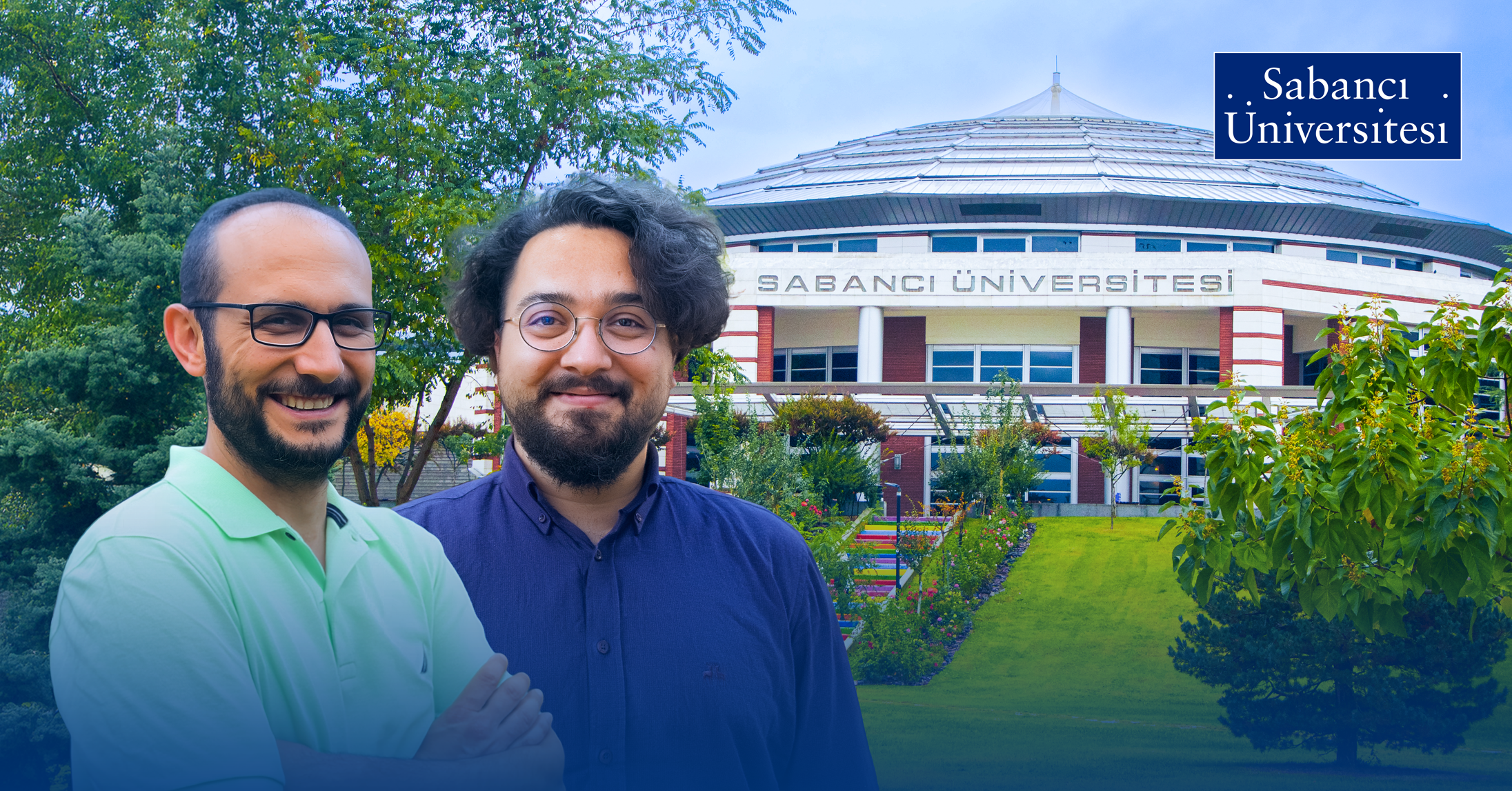
The CMOS 2.0 projects supported by IMEC will be supervised by our Faculty of Engineering and Natural Sciences faculty members Özcan Öztürk and Korkut Kaan Tokgöz.